Week 10: Input Devices
In this tenth week of Fab Academy, there are two types of assigments. The individual assigment is to measure something i.e.add a sensor to a microcontroller board that you have designed and read it.
The group assigment is to measure the analog levels and digital signals in an input device. Further learnings from this week are listed below:
- Probe an input device(s)'s analog and digital signals
- Read the datasheet for the microcontroller
- Program the board you have made depending upon the sensor used
- Explained the programming process used
- Explain the mistakes that I had made and how I corrected it
- Include hero shots of the board
- Document the interfacing between the input devices to microcontroller and how physical property relates to measured resutls
- Document the PCB Design and fabrication of the board
- Try out a cool experiments
The following are the softwares that I have used for learning various operations:
- Arduino IDE : Programming
- MIT Mods : Machine Management
Looking back to the previous electronic weeks, I am pretty nervous about whether the PCB routing would go as expected. For this week's assignment, I am planning to get my hands on IR Sensor Module which can be interfaced with the new custom board. The IR obstacle sensor is used for plethora of applications, ranging from sorting devices to missle guidance. Due to the lockdown, I had to combine the input week's and output week's board to complete the assigment on time.
| |
|
|---|---|
| Wednesday | Prof. Neil's class on Input Devices |
| Thursday | No Class |
| Friday | No Class |
| Saturday | Research |
| Sunday | Research |
| Monday | Designing the PCB and milling |
| Tuesday | Soldering, Programming and Testing |
I am pretty sure that I won't be able to complete this week's assigment due the break but I will try to complete it asap. My first agenda is to finish designing the board as soon as possible as the milling and soldering aspect may take time and will depend upon my slot. My idea for this week is to interface my board with an IR obstacle sensor module which is capable of detecting objects in front of it. The module is commonly used is robotic projects, railways, medical devices etc. When I think about this module, I remember that I had used this sensor during the freshman year of my college, where my team had made a line follower robot for a national level competition. We had used the IR array module but unfortunately we failed in the final level of the competition due to calibration issues. The below image shows a line follower robot, which is similar to the one that I had build long before:
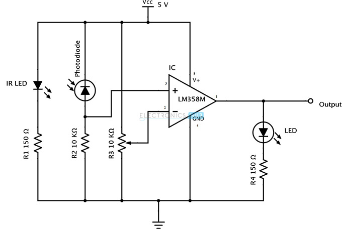
An infrared sensor is an electronic device, that emits in order to sense some aspects of the surroundings. An IR sensor can measure the heat of an object as well as detects the motion. These types of sensors measure only infrared radiation, rather than emitting it that is called a passive IR sensor. Usually, in the infrared spectrum, all the objects radiate some form of thermal radiation. These types of radiations are invisible to our eyes, which can be detected by an infrared sensor. The emitter is simply an IR LED (Light Emitting Diode) and the detector is simply an IR photodiode that is sensitive to IR light of the same wavelength as that emitted by the IR LED. When IR light falls on the photodiode, the resistances and the output voltages will change in proportion to the magnitude of the IR light received. Proximity Sensor are used to detect objects and obstacles in front of sensor. Sensor keeps transmitting infrared light and when any object comes near, it is detected by the sensor by monitoring the reflected light from the object. It can be used in robots for obstacle avoidance, for automatic doors, for parking aid devices or for security alarm systems, or contact less tachometer by measuring RPM of rotation objects like fan blades. The module features a 3 wire interface with Vcc, GND and an OUTPUT pin on its tail. It works fine with 3v3 to 5V levels. Upon hindrance/reflectance, the output pin gives out a digital signal (a low-level signal). The onboard preset helps to fine tune the range of operation, effective distance range is 2cm to 80cm. The properties of the module are as follows:
- Onboard detection indication.
- Effective distance range of 2cm to 80cm.
- A preset knob to fine-tune distance range.
- Detection angle: 35 °.
- Comparator chip: LM393.
The below image shows the IR Sensor Module that I am using for this week's assigment. I am using IR Sensor module based on transistor.
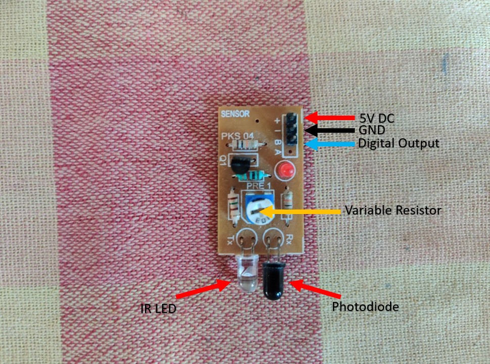
Structure and working of IR Sensor Module
An infrared sensor circuit is one of the basic and popular sensor modules in an electronic device. This sensor is analogous to human’s visionary senses, which can be used to detect obstacles and it is one of the common applications in real-time. This circuit comprises the following components. The sensor gives digital low as output when an obstacle is detected.
It consists of an IR LED, a photodiode, a potentiometer, an IC Operational amplifier and an LED. IR LED emits infrared light. The Photodiode detects the infrared light. An IC Op – Amp is used as a voltage comparator. The potentiometer is used to calibrate the output of the sensor according to the requirement. When the light emitted by the IR LED is incident on the photodiode after hitting an object, the resistance of the photodiode falls down from a huge value. One of the input of the op – amp is at threshold value set by the potentiometer. The other input to the op-amp is from the photodiode’s series resistor. When the incident radiation is more on the photodiode, the voltage drop across the series resistor will be high. In the IC, both the threshold voltage and the voltage across the series resistor are compared. If the voltage across the resistor series to photodiode is greater than that of the threshold voltage, the output of the IC Op – Amp is high. As the output of the IC is connected to an LED, it lightens up. The threshold voltage can be adjusted by adjusting the potentiometer depending on the environmental conditions.
The positioning of the IR LED and the IR Receiver is an important factor. When the IR LED is held directly in front of the IR receiver, this setup is called Direct Incidence. In this case, almost the entire radiation from the IR LED will fall on the IR receiver. Hence there is a line of sight communication between the infrared transmitter and the receiver. If an object falls in this line, it obstructs the radiation from reaching the receiver either by reflecting the radiation or absorbing the radiation.
Advanatages and disadvantages of IR Sensors
Advantages:
- It uses less power.
- The detection of motion is possible in the presence or absence of light approximately with equal reliability.
- They do not need contact with the object for detection.
- There is no data leakage because of the ray direction.
- These sensors are not affected by oxidation & corrosion
- Noise immunity is very strong
Disadvantages:
- Line of sight is required.
- Range is limited.
- These can be affected by fog, rain, dust, etc.
- Less data transmission rate.
Applications:
- Radiation Thermometers
- Flame Monitors
- Moisture Analyzers
- Gas Analyzers
- IR Imaging Devices
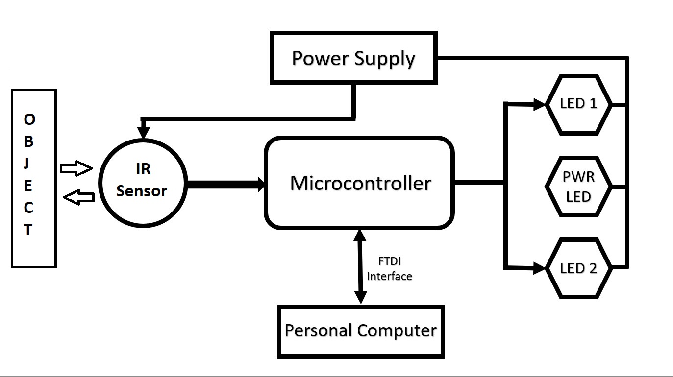
Before going to the steps involved in designing, I had made a rough block diagram to make it understand better for the people who visit my page. In this block diagram I am only including components required for this week and I will be making a seperate one for Week 12: Output devices even though both are included in same board. Based on diagram, the IR sensor which is the input device detects IR rays which sends signal to microcontroller and the microcontroller then actuates the LED which is the output device.
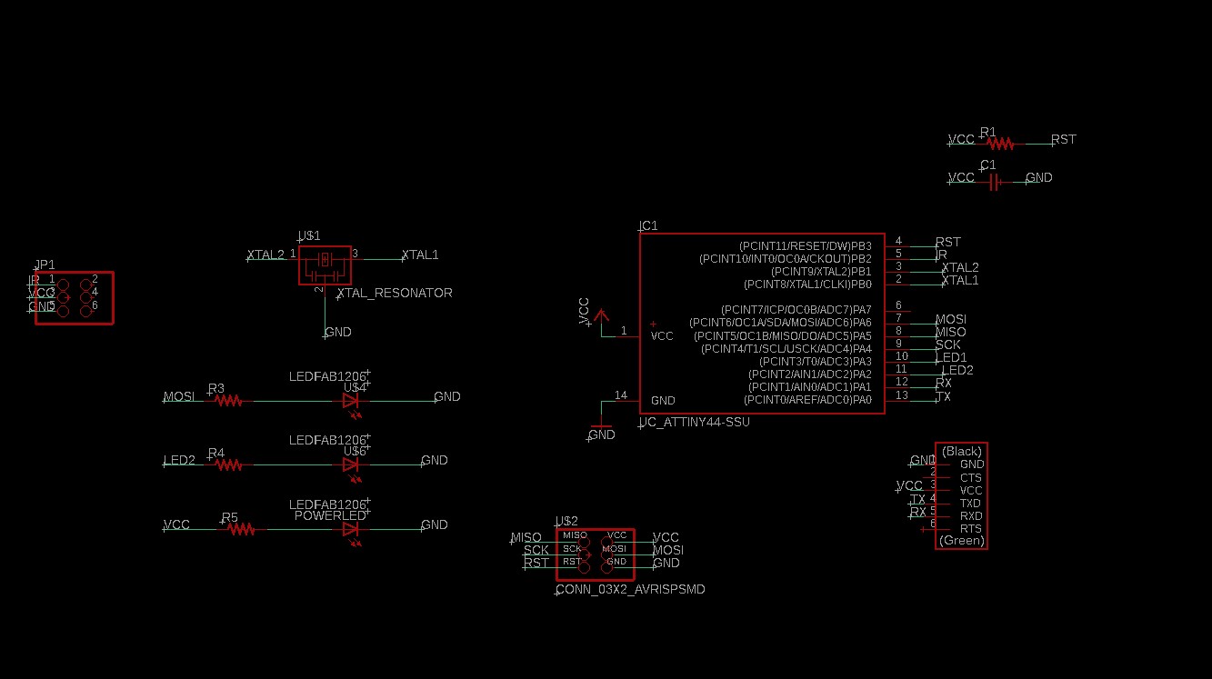
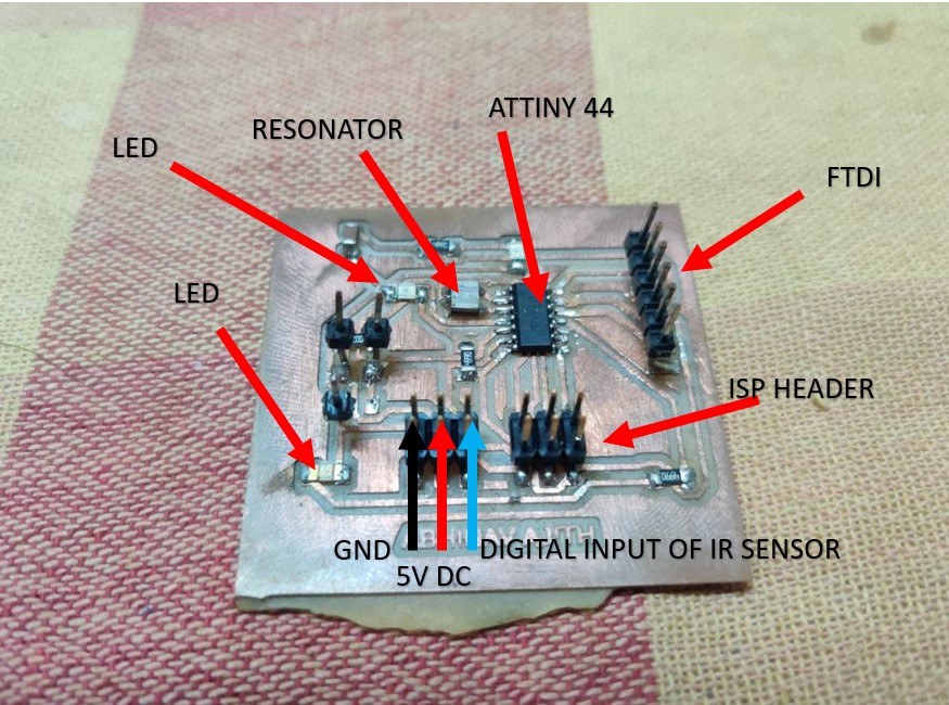
Following the steps mentioned in Week 6: Electronic Design, I had made the schematic of the board in Eagle. I had initally designed this board for phototransistor as the input device but due to erros that I had received using the sensor, I had switched to IR Proximity Sensor for this weeks assignment. Here the LEDs blink upon the actuation of the IR Sensor. The values are set in the programming for the LED to activate and deactivate. I had used ATtiny 44A as the microcontroller.
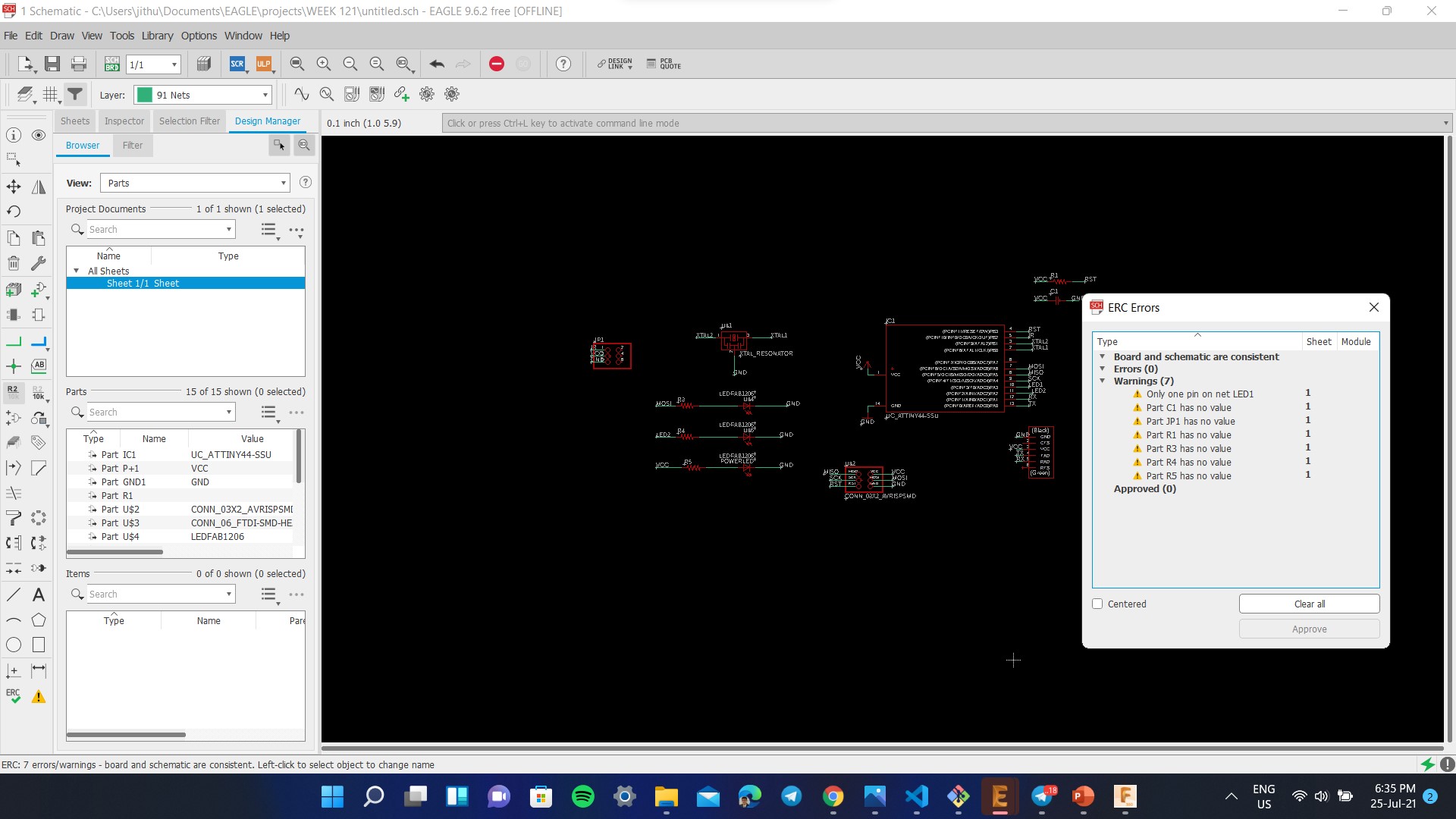
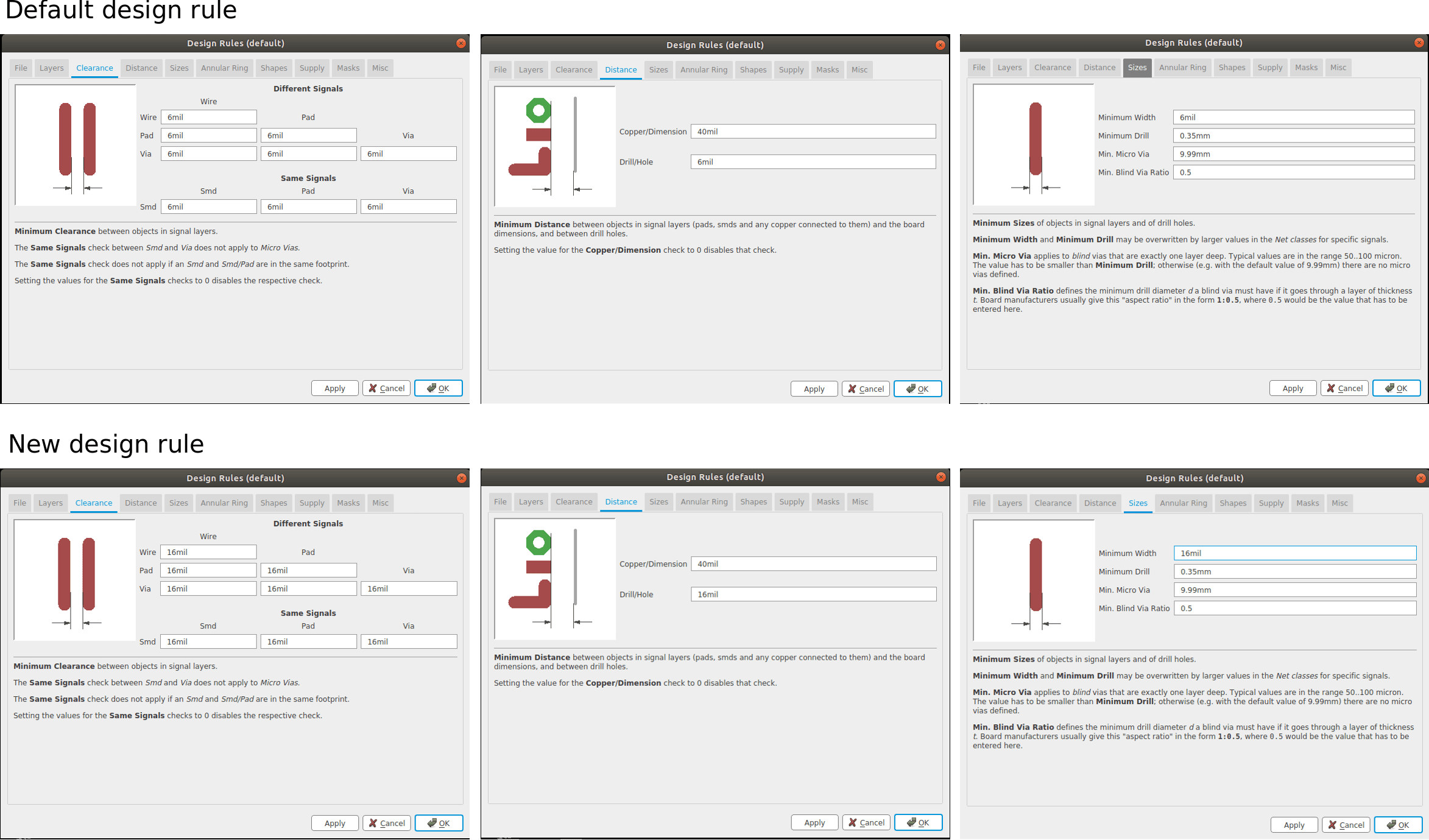
Then you need to place the components away from each other and checked whether the airwires cross each other. You need to rotate and move the components so that there is minimum crossing of airwires. As per the default setting the widths are set to 6mil. This thickness cannot be achieved using our Milling machine. The design rule can be changed from the 'Design Rule' in the 'Edit' option on the taskbar.
For routing the connection I used the 'AUTO ROUTE' tool. Fortunately my biggest fear was busted here, I got 100% routed circuit in my second try and I think this is a huge achivement for me since I now know about placing the components in respective locations to attain the best result.
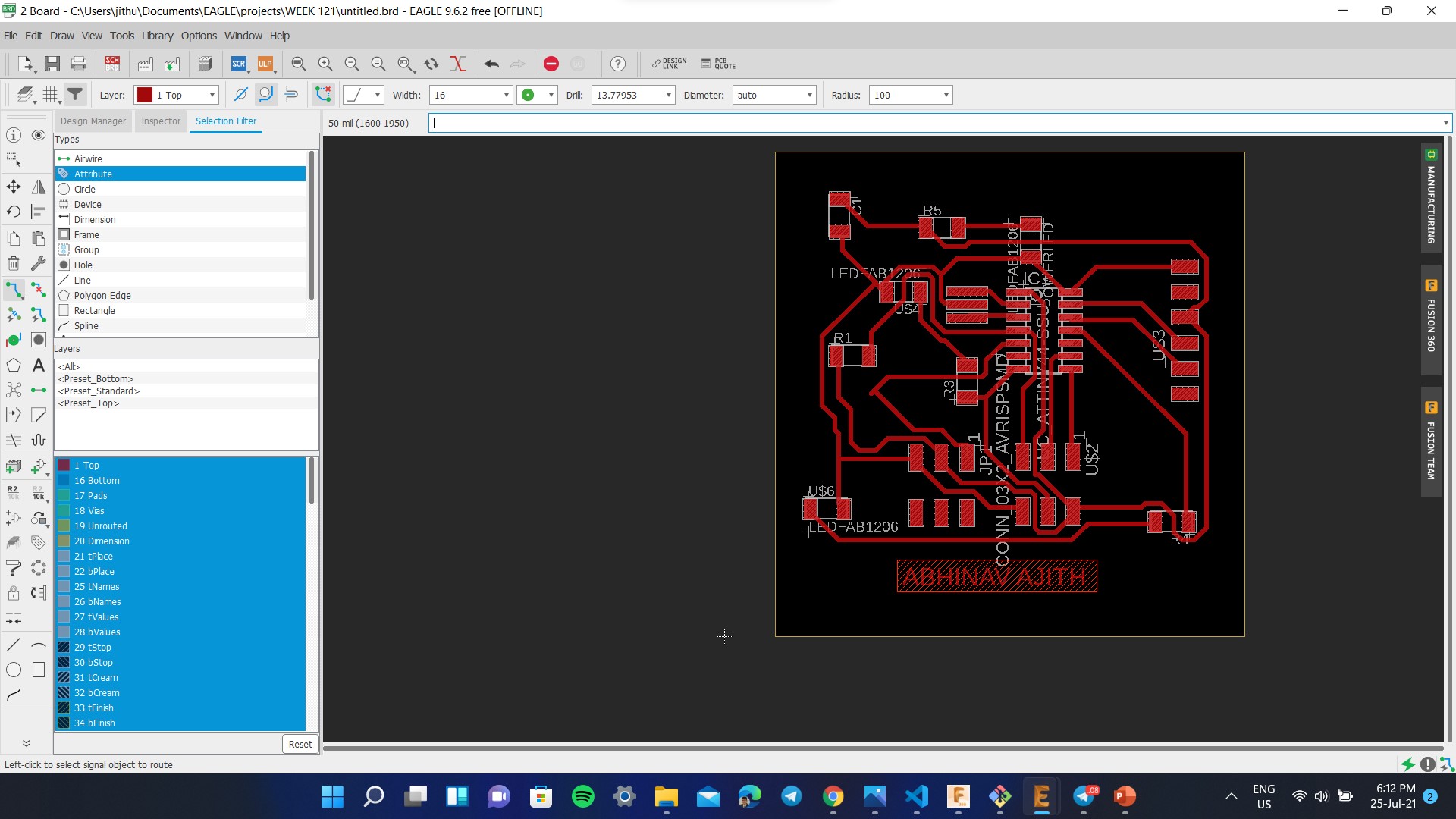
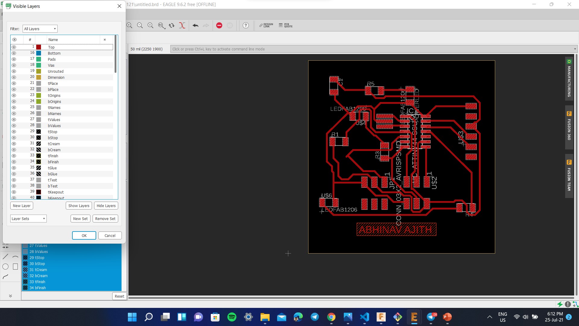
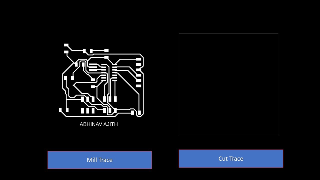
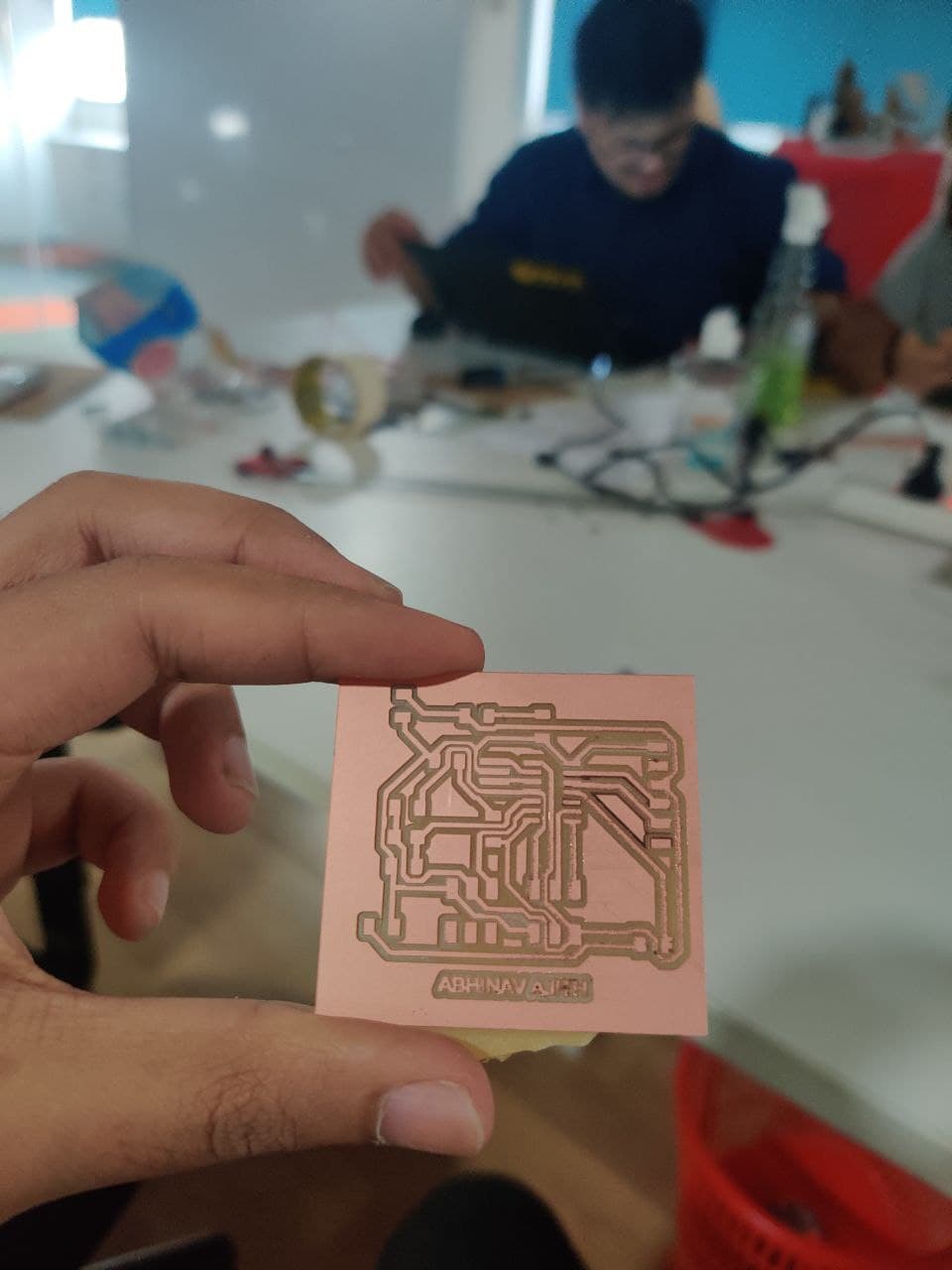
Since I missed this weeks class due to personal reasons, I tried to do this weeks work with Week 12: Output devices as a single board to reduce the machining time. The below image shows the final optimized circuit. The writings on the board design are for our understanding, These writtings must be eliminated before we give it for milling. So for eliminating the writings go to 'LAYERS SETTINGS' and on the 'VISIBLE LAYERS' window enable only the Top layer for the traces.
o disable the 'PAD NAMES' and 'SIGNAL NAMES' on the board design, go to 'OPTIONS' on the taskbar and select 'SETTINGS'. On the 'SETTINGS' window click on 'MISC' and disable the PAD NAMES and SINGNAL NAMES. To export the file design as png file, Go to 'FILE' on the taskbar and click 'EXPORT' and select 'IMAGE'. Then a window opens and browse the destination, make it monochrome and change the resolution to 1000dpi. These are the milling and cutting traces of the board
Milling the PCB using Modela PCB Milling Machine
Referring Week 4 you need to export the drawings to the MODS. Always mill out the Traces first using the 1/64 bit and change the tool to 1/32 bit and position the tool to the same origin used for tracing. Afer importing the image you need to calculate the bit and calculate raster. Ensure that you trace first followed by cutting. Once calculation is complete you can verify the tool path by selecting the view command. Next you need to set the origin by going onto suitable coordinates referred from the work area in the milling machine and don't ever forget to remember/screenshot the X & Y coordinates. You can repeat the same process for cutting as well but make sure that you use 1/32 bit and ensure that the origin coordinates are alike. The final step is to verify the origin and to send the file for milling by clicking on send from WebSocket Module. The next step is to clean the board using a vacuum cleaner after completing the whole milling process. Furthermpre, there will be some unwanted copper in the PCB which can be easily removed using a knife. These steps are depicted below
There were some human errors that occured during the milling process. I am listing them below:
- At first the copper was not milled properly, then I troubleshooted and found that the Z axis calibration was not properly done and I also forgot to check whether the surface was bent or not
- The bit went out from the surface of copper during cutting, which was caused due to improper calculation of the area required for the PCB
The next step is to list out all the components required for the project. The bill of components are as follows:
- ATtiny 44 - 1
- XTAL 20 KHz Resonator - 1
- IR Proximity Sensor Module - 1
- ISP Header (3*2) - 2
- FTDI Header - 1
- 10K Ohm Resistor - 2
- 499 Ohm Resistor - 3
- LED - 3
- 1 Micro Farad Capacitor - 1
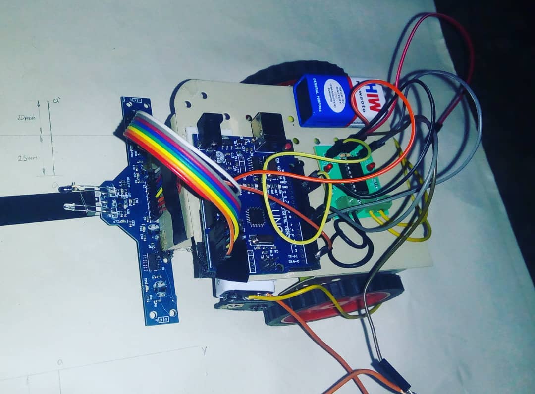
The next step is to solder the components and test whether the board works or not. The board initally had some issues with the pins so I added custom male pins to test the same. The image of soldered PCB is shown below:
The below image shows the connection between the custom board and the IR sensor module.
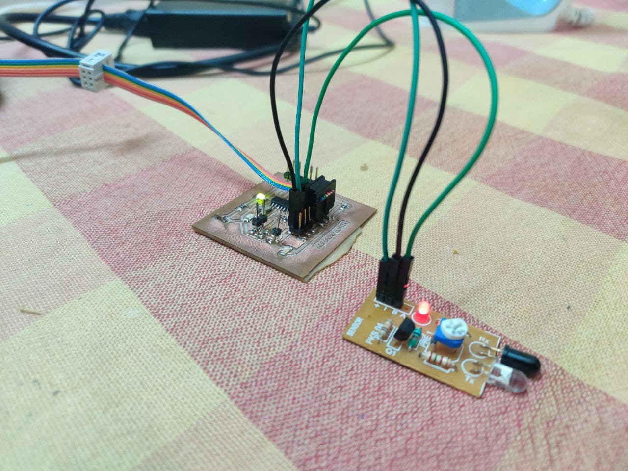
There were lot of errors that arouse after the completion of the board. The main issue was with the quality of jumper wire that I had and it had created a lot of unncessary errors which was finally found out and solved. Furthermore proper cleaning of the board was required for perfect operation.
This is the tough part in this week, there is no use building the board if it doesn't work as expected. Due to the lockdown, I shifted to Fablab Trivandrum where the components are limited. So I had initally designed the board for ATtiny 45 but I had used ATtiny 44A in the board. The idea was to detect the presence of an object in front of the proximity sensor and it will be reflected in the custom board as LED output. Here is the Arduino code that I had used:
void setup()
{
  pinMode(PA6,OUTPUT); //Setting the pin for LED
  pinMode(PB2,INPUT);  //Setting the pin for IR Sensor

}
void loop()
{
  if (digitalRead(PB2)== LOW)  //If there is an obstacle detected
  {
    digitalWrite(PA6,HIGH);  //LED will turn on

    delay(10);
  }
  else
  {

    digitalWrite(PA6,LOW); //Else LED will not glow
    delay(10);

  }

}
The code worked as expected after several trials and I was happy to see the sensor working without fail. The below video shows the working of the sensor:
This week's group assignment is to probe an input device's analog levels and digital signals. Here I had used my board to measure the digital signals based on output from IR Sensor. The variation can be seen in the video.
            #include <.SoftwareSerial.h>
            int sensorPin = PB2;
            int digitalValue = 0;
            SoftwareSerial Serial(0, 1);
            void setup()
            {
             pinMode(sensorPin,INPUT_PULLUP);

             Serial.begin(9600);

            }
            void loop()
            {
            digitalValue = digitalRead(sensorPin);
               Serial.print("Digital Value ");
             Serial.println(digitalValue);
             delay(1000);
            }
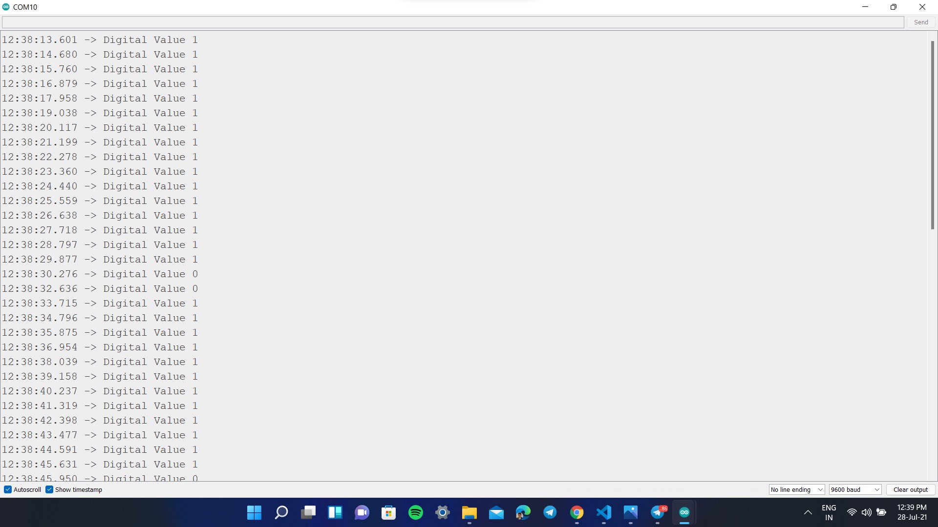
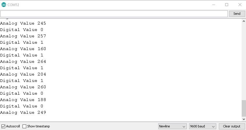
I also confirmed the same using a DSO. The group assigment although was done alone, was very interesting to do and I specially thank my lab supervisor Vinod Kumar for helping me when I was stuck. I am including the video of DSO signals below: 9
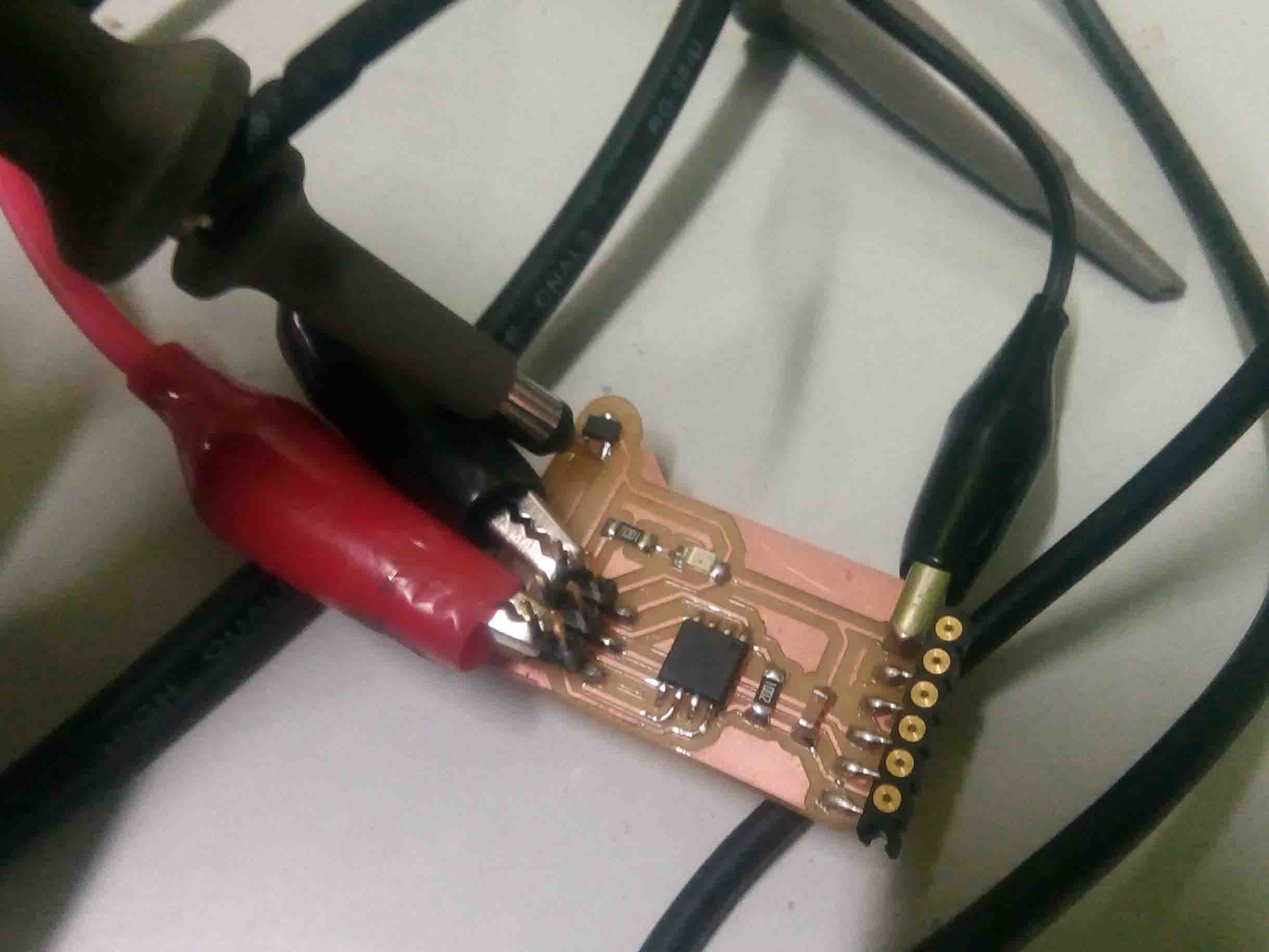
Since my pin that I had used for IR Sensor doesn't support Analog signals, I had used a random board that was available in the lab to check the signals. The board that I had used has a hall effect sensor which is connected to Pin 1 (PB5) of a Attiny 45. Since the port has analogue readings enabled, I got the values correctly.
                #include <.SoftwareSerial.h>
                int sensorPin = PB5;
                int digitalValue = 0;
                int analogValue = 0;
                SoftwareSerial Serial(0, 1);
                void setup()
                {
                 pinMode(sensorPin,INPUT_PULLUP);

                 Serial.begin(9600);

                }
                void loop()
                {
                digitalValue = digitalRead(sensorPin);
                  analogValue= analogRead(sensorPin);
                   Serial.print("Digital Value ");
                 Serial.println(digitalValue);
                 delay(1000);
                  Serial.print("Analog Value ");
                 Serial.println(analogValue);
                 delay(1000);
                }